Monday, May 11, 2009

Laser Marking on Ceramic Application

The parts were laser marked using a 20 watt q-switched ytterbium fiber laser with 160 mm focal length lens. The parts were surface marked to create brightly contrasting marks. The parts were marked using various parameters, resulting in various cycle times and various darknesses and qualities of marks on the samples.
"Fonon Display and Semiconductor marking and engraving products range from smaller handheld systems to larger industrial sized machines," said Maureen McHale, Fonon Display and Semiconductors Corporate Marketing and Public Relations Manager. "This ensures no matter the size of the company or application Fonon DSS can provide an affordable system which is easily integrated into any production facility," continued McHale.

Thursday, May 7, 2009

Medical Device Marking Using a Fiber Laser

The parts were marked on this medical saw using a 20Watt Fiber Laser Marking System. The parts were marked with a single line, narrow font for speed purposes and a bold font to increase readability. The parts were engraved deep enough that the marking would very hard to remove. One part was engraved using a narrow font, this produced a short cycle time. The cycle time for narrow engraved part took 3 seconds. The second part was engraved with a bold font to increase readability; the cycle time for the bold font was 8.5 seconds.

For more information, visit our website!

Looking for a new laser system? Send us your samples...
Our experienced staff of applications engineers are familiar with a wide variety of applications across many different manufacturing industries. Send us several samples of your product with a complete description of your marking or cutting requirements. Your processed parts, together with a detailed applications report and equipment recommendations will be returned to you at no charge. FREE SAMPLE PROCESSING

Wednesday, May 6, 2009

Marking Glass Using a CO2 Laser


The light bulb glass was marked using Synrad 48-2 25 watt CW CO2 laser with a FLA125 focal length lens. The glass was marked using a power of 25 watts at a speed of 25” per second, resulting in a cycle time of 0.52 seconds. The font was a simple stroke. The material provided readable marks.


Looking for a new laser system?

Our experienced staff of applications engineers are familiar with a wide variety of applications across many different manufacturing industries. Send us several samples of your product with a complete description of your marking or cutting requirements. Your processed parts, together with a detailed applications report and equipment recommendations will be returned to you at no charge. FREE SAMPLE PROCESSING

Tuesday, May 5, 2009

Blackstar SW300 Cutting Solar Silicon Panels

BLACKSTAR™ is a Wafer Dicing System utilizing Fantom Width Laser Dicing Technology® (FWLDT®) invented and patented by Fonon Technology and modified to accommodate the requirements of a silicon wafer singulation process without affecting the existent dicing method, processes or procedures.

Wafers have the highest value at the dicing stage and the primary focus of a BlackStar™ is to increase the number of dies, yield per wafer, and to maximize throughput while minimizing the HAZ specifically for “power hungry” RF micro devices and low-K wafer substrates.

The system is applicable for dicing of assorted semiconductor materials such as silicon (Si), gallium arsenide (GaAs), germanium (Ge), indium phosphide (InP), silicon carbide (SiC), gallium nitride (GaN), gallium phosphide (GaP), other compound materials, as well as low-k and multi-layer composite materials.

BlackStar™ is an alternative to mechanical saws too damaging and costly for cutting of thin delicate silicon, low-K and complex material wafers.

Watch the BlackStar™ in Action Now!

Friday, May 1, 2009

Brittney Spears Guide to Semiconductors?

If you haven't already stumbled on this site...
"Britney Spears' Guide to Semiconductor Physics" maybe it's time, after all...it's Friday!


According the to authors...
"It is a little known fact, that Ms Spears is an expert in semiconductor physics. Not content with just singing and acting, in the following pages, she will guide you in the fundamentals of the vital semiconductor laser components that have made it possible to hear her super music in a digital format."

Enjoy and have a great weekend!

Friday, April 24, 2009

TFT Film Cutting

Fonon Technology International, Inc., the world-renowned inventor and manufacturer of equipment based on ZWLCT® (Zero Width Laser Cutting Technology®) offers the latest innovation in laser scribing for the FPD (Flat Panel Display) Industry, the Fantom™ product line. Offering a stand-alone system for scribing TFT LCD panels, based on a C3 Laser™ Integrated Glass Scribing Laser Module, the Fantom™ series of laser scribing systems are cable of scribing glass panels ranging in size from Generation 3 to the large format Generation 8.


Watch the TFT Film Cutting Video NOW!
http://www.fonondss.com/video_tft_film_cutting.html

Wednesday, April 22, 2009

Fonon DSS' Update on TFT LCDs

As of 2008, all color LCD TVs and monitors use thin-film transistor liquid crystal displays (TFT LCDs). Coincidently, the best known application of thin-film transistors is in TFT LCDs. In this process, transistors are embedded within the panel itself, reducing crosstalk between pixels and improving image stability. The most beneficial aspect of TFT technology is a separate transistor for each pixel on the display. As each transistor is small, the amount of charges essential for controlling it also small. This allows for very fast re-drawing of the display. Prior to TFT, passive matrix LCD displays could not keep up with fast moving images. A mouse dragged across the screen, for example, from point A to point B, would disappear between the two points. A TFT monitor can track the mouse, resulting in a display that can be used for video, gaming and all forms of multimedia.

The Future of TFT LCDs
As the world still struggles to determine if we’re in a recession, depression or none of the above, some industries are showing signs that the worst of whatever ails us, although may not be completely over, is starting to show signs of improvement. The flat panel display industry, for one, seems to have reached the bottom of the cycle back in February 2009 and now the latest survey results are showing some recovery.

According to the March 2009 DisplaySearch report, shipments of large-area TFT LCD panels reached 37.9 million units, showing strong month over month growth of 29%. Additionally, large-area TFT LCD revenues reached $3.9 billion, up 31% month over month and all three major applications—notebook PC, monitor and TV—showed over 20% month over month growth, and total shipments were the highest in six months.

“As the FPD industry starts to rebound, businesses should be looking at using technology to improve their manufacturing operations during these tough economic times so that when the market does fully recover – they’re already ahead of the game.” This is according to Maureen McHale the Corporate Marketing and Public Relations Manager for Fonon Display and Semiconductor Systems (Fonon DSS). “This is a time for innovative thinking and for manufacturers to take advantage of the current economic situation by improving processes, updating equipment and implementing cost saving technology," she explained.

Laser Equipment for the FPD Industry
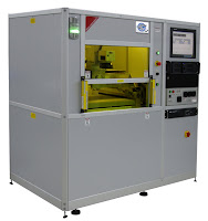
Fonon DSS has developed laser equipment for the flat panel display (FPD) industry which is used in helping to create very thin display screens for portable computers, T.V. screens, radio faces, and most LCD technology. Flat panel display technology has become increasing popular over other existing technologies because the display is thinner, lightweight and more power efficient. Manufacturing this high tech product requires equally high tech equipment like fiber laser systems which are not only able to produce high quality results, they can lower manufacturing costs and increase throughput.

Fonon DSS’ turnkey equipment is designed and built utilizing cutting-edge technology and patented methods including Zero Width Laser Cutting Technology (ZWLCT®). This new industrial method uses a laser controlled power density profile on the material surface to generate the subsurface forces greater than intermolecular connections. The methodology utilizes a non-contact laser induced internal stress to produce a controlled separation. Since the technique is non-contact, the surface degradation associated with mechanical scribe and break is eliminated, thus removing the need for additional cleaning of the glass. Yield loss as a result of particulate damage is also greatly reduced. This technique has the highest level of precision known to man and it has dramatically improved the substrate separation process, specifically for latest generations (Gen 6, 7, and 8) glass panels for Flat Panel Display (FPD) manufacturing.

In order to utilize the patented ZWLCT® for laser scribing glass for the FPD industry, Fonon DSS has incorporated this technology into the latest innovation, the Fantom™ product line. These stand-alone systems have been built for scribing TFT LCD panels, utilizing a C3 Laser™ Integrated Glass Scribing Laser Module. Fonon DSS' Fantom™ laser scribers are designed to increase efficiency providing higher throughput rates and continually proving to be the more cost effective solution.


Discover the Fantom™ Advantages:

The Fantom™ product line offers many advantages over traditional, more costly methods as outlined here:
1) In comparison to the older method of glass cutting, the cost of ZWLCT® technology continues to decrease, while mechanical scribing systems increase. As panel sizes increase the cost of mechanical equipment grows exponentially with each increase in panel size, while laser equipment costs only increase linearly. This change in market ROI makes Fonon DSS' laser scribers and ZWLCT® methods the clear choice when comparing cost factors.


2) Fonon’s patented glass scribing technology surpasses the older mechanical technology used to cut glass and other brittle materials for the electronic and semiconductor industries. Conventional technology creates vent cracks by stressing the substrate, which in turn creates surface damage and lateral cracks, resulting in particulate generation, and yield loss. It is this loss, plus the purchase cost for mechanical scribing and breaking systems, that has become the significant contributor to the retail cost of modern flat panel displays.

3) The Fantom™ scribing systems utilize ZWLCT® which allows scribing applications to be processed with tremendous speed, no material loss, and no chips or other debris associated with conventional scribe and break techniques thereby eliminating the cleaning and grinding line.
Enhancements are continually being made to ZWLCT® methods and the Fantom™ line - growing and changing with the industry, allowing manufacturers to reduce costs and increase production. For more information about Fonon DSS’ Fantom™ laser scribing systems and more laser equipment, please visit http://www.fonondss.com/ or call 407-829-2613.

Fonon DSS, the cutting edge developer of state-of-the-art, laser scribing, dicing, marking, coating removal, direct patterning, and photo mask repair solutions for the Flat Panel Display (FPD), Semiconductor, Photovoltaic and Electronics industries throughout the world.
Media Contact:
Maureen McHale
mmchale@fonondss.com
407-829-2613 x317

Monday, April 20, 2009

The Fiber Laser Advantage to Chip and Wafer Marking

Marking chips and wafers is a requirement for manufacturers within the semiconductor, flat panel display and solar panel industries. Fiber laser systems can apply computer-generated images such as bar codes, serial numbers, logos, and UID marks to a wide variety of metallic and nonmetallic materials. In the chip and wafer manufacturing process, such marks are the key to traceability and improving production processes. Direct fiber laser marking is becoming widely accepted as the best solution.

As an advancement to traditional ink marking, the nd:YAG laser was the earliest laser to be used for wafer marking. The nd:YAG laser is still the most common in the industry; however, manufacturers are now, more than ever, focused on improving processes to reduce costs and increase throughput, thereby increasing profitability. The lower cost of ownership (COO) and higher throughput of fiber laser marking systems compared to the YAG laser and traditional ink marking makes fiber laser systems very appealing.

Lower Costs, Higher Throughput
Manufacturing and material processing equipment can be very expensive; especially when your process contains two or more different applications. A unique benefit of fiber laser systems is that one laser can operate different processes with the use of an optical switch. For example, a manufacturer can operate cutting, marking and welding machines all off of the same fiber laser. This is especially beneficial to companies who are experiencing growth or looking to move into different processing markets.

As production increases or new applications need to be implemented a manufacturer can also upgrade their laser wattage easily and affordably. Since the laser itself is the most expensive component of a system, manufacturers can save a considerable amount of money while expanding their operation in a more exponential manner. Additionally, the average diode life for Co2 and nd:YAG lasers is approximately 10,000 to 20,000 hours. Fiber lasers have an astonishing 50,000 to 100,000 hour diode life. A longer diode life, means less maintenance and less down time to change out the diode allowing your production to continue.

Compared to Co2 and nd:YAG laser systems, fiber laser systems do not require the use of consumables in their operation and are approximately 20 times more energy efficient. Both of these factors not only help manufacturers become more eco-friendly but are also key to reducing operating costs.

Production speed and throughput is a major concern for most manufacturers. The combination of speed, performance and versatility of fiber laser systems cannot be matched by any other marking technique. Fiber lasers offer high throughput due to the fiber-to-fiber architecture presenting a robust, monolithic design with no optics to align or maintain, no mechanics to stabilize, and high power densities are able to process even the most demanding applications. This allows manufacturers to increase the rate they process materials while not having to compromise any quality.

Semiconductor Industry Applications
Portable digital components, cell phones, PDAs, and digital cameras become smaller and more lightweight but continue to increase in functionality. The Direct Chip Attach (DCA) or flip chip produces a need for wafer identification and tracking. Laser marking a wafer before it has been diced and processed enables manufacturers to trace defective parts. Due to the ever shrinking size of chips, the ability of a fiber laser to produce a small spot size weighs in heavily. Utilizing laser marking, as opposed to ink marking, is the best solution because it provides a mark that is permanent, readable, and of a enough high quality to meet even the most stringent requirements.

Flat Panel Display Industry Applications
Traditional methods to mark glass panels with tracking codes such as mechanical etching can crack the surface of the glass thereby compromising the overall strength and quality of the glass. These cracks can potentially lead to panel issues in the future. Additionally, the marks are not always clear enough to be scanned or easily read. Although laser marking technology has been around since the 1970s, it has been slow to replace traditional methods. But, the combination of speed, permanence, and reliability, is making manufacturers stand up and take notice when high throughput, time savings and lower costs are clearly the focus for flat panel display manufacturers.

Solar Industry Applications
Typically, consumers require 20 to 25 year warranties on solar panels. Therefore, wafer marking in solar cell manufacturing for traceability is a must. Traditional methods to mark panels with tracking codes such as mechanical etching or engraving using a Co2 laser can crack or chip the surface of the glass thereby compromising the overall strength and quality of the glass. Due the harsh environments the panels must endure, these imperfections can potentially lead to panel issues in the future affecting panel longevity.

Overall, fiber laser marking has proven to be the best solution to chip and wafer manufacturers, because it produces a permanent, readable, and high quality mark fulfilling manufacturers marking's most stringent requirements. And finally, the lower cost of ownership (COO) and higher throughput of fiber laser marking systems can’t be ignored in these tough economic times.

Fonon DSS, the cutting edge developer of state-of-the-art, laser scribing, dicing, marking, coating removal, direct patterning, and photo mask repair solutions for the Flat Panel Display (FPD), Semiconductor, Photovoltaic and Electronics industries throughout the world. For more information about Fonon DSS’ systems, please visit http://www.fonondss.com/ or call 407-829-2613.

Media Contact:
Maureen McHale
mmchale@laserphotonics.com
407-829-2613 x317

Wednesday, March 25, 2009

Semiconductor Online Features Fonon DSS!

Semiconductor Online featured Fonon Display and Semiconductor Systems new invention -Laser Direct Writing! To read the complete article, click on the logo below:


Friday, March 20, 2009

Fonon DSS Invents Laser Direct Writing

Fonon DSS (Display & Semiconductor Systems), the innovative developer of state-of-the-art, laser scribing, dicing, marking, coating removal, direct patterning, and photo mask repair solutions for the Flat Panel Display (FPD), Semiconductor, Photovoltaic and Electronics industries throughout the world announced the invention of Laser Direct Writing for tracking glass panels.

Traditional methods to mark panels with tracking codes such as mechanical etching or engraving using a Co2 Laser can crack the surface of the glass thereby compromising the overall strength and quality of the glass. These cracks can potentially lead to panel failure issues in the future. Additionally, the marks were not always clear enough to be scanned or read.

Laser Direct Writing is a non-destructive, patent pending laser marking technology which marks glass without damaging the surface while producing a readable image. This process does not require tapes or sprays to make the mark thereby eliminating any cleaning and post processing required with other methods.

“Panel manufacturers have been looking for a better way to mark panels with bar codes and UID marks,” said Maureen McHale, the Corporate Marketing and Public Relations Manager for FononDSS. “Laser Direct Writing creates a black, semi-transparent or gold marking on glass and is ideal for tracking the life of the panel. This process does not damage the glass and ensures readability of the mark.”

Fonon DSS, the cutting edge developer of state-of-the-art, laser scribing, dicing, marking, coating removal, direct patterning, and photo mask repair solutions for the Flat Panel Display (FPD), Semiconductor, Photovoltaic and Electronics industries throughout the world. For more information about Fonon DSS’ systems, please visit http://www.fonondss.com/ or call 407-829-2613.


Media Contact:


407-829-2613 x317

Monday, February 16, 2009

IC Chip Failure Analysis System - the FiberTower DFAS


Fonon DSS (Display & Semiconductor Systems), the cutting edge developer of state-of-the-art, laser scribing, dicing, marking, coating removal, direct patterning, and photo mask repair solutions to the Flat Panel Display (FPD), Semiconductor, Photovoltaic and Electronics industries throughout the world announced today the release of the improved FiberTower™ DFAS IC chip package failure analysis system.

The FiberTower™ DFAS uses laser technology to allow an operator to remove individual layers of the mold compound all the way through to the substrate. The DFAS operator can chose to remove the entire compound, individual layers, or sections of the mold compound ranging from the entire sample to just one wire due to the precision of the laser spot positioning. The FiberTower™ DFAS can import images from a variety of testing processes such as SAM, X-Ray, and SEM to show the operator exactly the area of concern within the sample.

Most failure analysis labs use time consuming chemical and mechanical etching processes on a routine basis to dissect chips to see why they failed. Unlike the uncontrollable, wet, chemical etch process, the DFAS IC chip decapitation process is 100% controllable by the operator through a Graphic User Interface (GUI). Utilizing the laser equipped DFAS, the operator can select a specific area to examine instead of dissecting the whole chip as chemical and mechanical etchers must do.

Traditionally, diamond saws were used for processes commonly used in failure analysis. This process is very slow requiring a significant amount of time for additional polishing due to the large standoff required from the cut, and still does not guarantee that the sample will not be damaged. The DFAS utilizes a Fonon’s laser wafer ablation process to provide an extremely accurate dissection without damaging the sample.

The FiberTower™ DFAS also offers a laser spectrometry option to provide a detailed report of all the materials as they are being processed. This feature allows the operator to find inconsistencies within the compound, flow settlement, and contaminants, and provides detail report of the exact characteristics of the mold compound. Improvements to the FiberTower™ DFAS include the use of scan servos with position feedback for higher accuracy and scan see through capabilities for on time inspection.

Eliminating the majority of cost, sample damage, as well as long term health hazards associated with the use of chemicals, the DFAS performs chip failure analysis with unmatched safety, savings, accuracy and speed.

About Fonon DSS: A division of Fonon Technology International, the world renowned inventor and manufacturer of Zero Width Laser Cutting Technology™, Fonon DSS focuses on the semiconductor and flat panel display industries utilizing the patented Zero Width Laser Cutting Technology™ (ZWLCT™) to create products with the highest level of precision. Fonon DSS provides state-of-the-art laser scribing, laser dicing and fiber laser marking solutions to customers in the Flat Panel Display (FPD), Semiconductor and Electronics industries throughout the world. For more information, visit http://www.fonondss.com/ or call 407-829-2613.

Monday, February 9, 2009

Zero Width Laser Cutting Technology™ (ZWLCT™)

Fonon Technology International has developed a completely new industrial method known to the world as Zero Width Laser Cutting Technology™ (ZWLCT™). The ZWLCT™ technique uses a laser controlled Power Density profile on the material surface to generate the subsurface forces greater than intermolecular connections. Our patented Zero Width Laser Cutting Technology™ (ZWLCT™) has the highest level of precision known to man. This technology has dramatically improved the substrate separation process, specifically for latest generations (Gen 6, 7, and 8) glass panels for Flat Panel Display (FPD) manufacturing.

The methodology utilizes a non-contact laser induced internal stress to produce a controlled separation. Since the technique is non-contact, the surface degradation associated with mechanical scribe and break is eliminated. Yield loss as a result of particulate damage is also greatly reduced. Cutting substrates in clean room conditions becomes feasible with ZWLCT™ leading to the ability to introduce a production line concept into clean room substrate manufacturing. This has not been possible before because of debris generated during cutting and edge grinding which will not be generated during ZWLCT™ processing. In addition, cleaning facilities can also be substantially reduced. These factors offer a cost effective solution to manufacturing space and efficiency.

Our latest mathematical modeling and empirical data gathering resulted in the development of an improved method and the requisite industrial machinery to enable us to introduce these improvements into the FPD industry. With this new method we can create internal tensile forces so great that we can achieve total separation of display type glass WITHOUT COOLING. Under these conditions the MicroCrack™ would propagate in the glass body at a depth of more than 0.7 mm (for bare glass). This process is called Full Body Separation.

The ZWLCT™ method incorporates cooling of the glass surface following controlled heating, with the correct power density profile, this creates the intermolecular separation of the glass substrate to a certain depth. Depth ( t ) has an inverse relation to the speed ( v ) of cutting, assuming that power ( P ) is constant. This means that the slower the speed the deeper the MicroCrack™ that is formed. Both mathematical models and empirical data support these conclusions and field experience has verified these findings.

Zero Width Laser Cutting Technology™ is the only technology available in the world with a NON DIMENSIONAL cutting line. The waste material by the cutting process is totally eliminated.

Friday, February 6, 2009

Glass Wafer Dicing Technology

As a result of exposure in camera windows and IR filter devices Fonon developed a precision separation of glass panels into individual components with the Zero Width Laser Dicing Technology®.

The ZWLDT® splits materials at the molecular level at tremendous speed with no material loss. This results in the highest edge quality and the fastest dicing speed.

Integrated scribe and break equipment is available for 100 x 100 mm, 200 x 200 and 300 mm in diameter glass substrates mounted on a standard 300 mm wafer hoops.

Quick Release tape made it possible to remove individual substrates from the dicing tape without the edge damage with Pick and Place equipment.

Laser dicing system showing below is a special machine designed for precise dicing of glass wafers.

The Glass Wafer Dicing Process:
  • Mount low-tack and quick-release tape on the metal tape frame
  • Laminate the substrate on the tape
  • Dice the substrate into specified-dimension dies with advanced Zero Width Laser Dicing Technology®
  • Apply a cover film
  • Flip upside down
  • Break with a metal bar
  • Expand on stretcher
  • Remove individual substrates from dicing tape without edge damage with Pick Place equipment

Applications:

  • Bio ID devices
  • Cell Phone Cameras and Display Panels
  • TFT & LCD Cells
  • CCD & IR camera windows
  • IR cut off filter
Advantages:
  • Higher speeds
  • Higher throughput
  • High precision and accuracy
  • No material loss
  • Shortens process and can be brought into clean room
  • Edges have a high resistance to breakage

Thursday, February 5, 2009

Silicon Wafer Dicing Technology

Wafers have the highest value at the dicing stage and the primary focus of a ZWLDT® is to increase the number of dies, yield per wafer, and to maximize throughput while minimizing the HAZ specifically for “power hungry” RF micro devices and low-K wafer substrates.

Fonon DSS System is applicable for dicing of assorted semiconductor materials such as silicon (Si), gallium arsenide (GaAs), germanium (Ge), indium phosphide (InP), silicon carbide (SiC), gallium nitride (GaN), gallium phosphide (GaP), other compound materials, as well as low-k and multi-layer composite materials.

BLACKSTAR™ series of a Wafer Dicing Systems utilizing a basic Zero Width Laser Dicing Technology® (ZWLDT®) invented and patented by Fonon Technology modified to accommodate the requirements of a silicon wafer singulation process without affecting the existent dicing method, processes and procedures.

The possibility of a cut with zero or 20 micron narrow width (application specific) allows wafer layout designers to reduce the width of the spacing between adjacent die on a wafer. The spacing is normally reserved to allow for the width of the saw used to cut the wafer. A reduction of the spacing width will result in an increase of the real estate available for die, which will result in a significant reduction of the cost per die.

The elimination of particles, debris and cutting fluids converts wafer dicing and separation into a “clean” operation. In certain areas of technology, i.e. MEMS, this attribute can almost be considered an enabler, since it will be possible to cut these devices without generating particles, which can damage these micro-mechanisms.

In addition, the elimination of cleaning steps and processing of cutting fluids introduces additional cost savings in the overall component fabrication process.

The elimination of wear items and consumables such as saw blades and scribes and the increased reliability associated with non-contact cutting versus a mechanical process, greatly decreases the cost of ownership of the equipment for the end-user.

Fonon’s Technology enables high-yield dicing and scribing of new materials, complicated layer stacks, and thin wafers including wafers with low-k dielectric and wafers with brittle material layers such as glass or silicon.

Significant Advantages of FTI's Dicing and Separation Technology:
  • Dicing thin silicon with high mechanical integrity and no chips.
  • Higher yield for thin wafers.
  • No Micro-Cracks, fragmentation or chipping even for silicon below 100µm thick.
  • Dicing wafers with thick polymer layers such as wafer scale packages and alpha barriers.
    No or minimal material loss means more parts per wafer (210 instead of 120 with mechanical saw).
  • High precision allows for smaller street width. Minimized Heat Affected Zone (HAZ).
  • BlackStar™ is an alternative to mechanical saws too damaging and costly for cutting of thin silicon, low-K, and complex material wafers.

Wednesday, February 4, 2009

Product Update: The Fantom G8™ - Cost Savings Uncovered

Fonon Display and Semiconductor Systems’ Fantom G8™ utilizes Zero Width Laser Cutting Technology™ (ZWLCT™) which allows scribing applications to be processed with tremendous speed, no material loss, and no chips or other debris associated with conventional scribe and break techniques. Additionally, ZWLCT™ maintains the integrity of the glass, making it three to five times mechanically stronger.

The Fantom G8™ splits materials at the molecular level with tremendous speed, no material loss, and no chips or other debris associated with conventional scribe and break techniques, it is ideal for ultra thin and larger G8-G11 size panels”, said Demitri Nikitin, CEO of Fonon Display and Semiconductor Systems. “Plus, the cost savings on the Fantom G8™ are tremendous and our prices not only include installation, but startup, and training as well.”

Consider the Savings:
  • The Fantom G8™ is a low cost solution for precision glass scribing priced the same as or less than precision mechanical scribers.
  • The Fantom G8™will produce glass panels without any additional edge processing, eliminating the grinding and cleaning line.
  • The Fantom G8™ features adjustable loading and unloading positions for in-line integration saving valuable processing time.
  • The Fantom G8™ is “plug-n-play”. It’s easy to install, quick to start-up and its operators training requirement levels are reduced.
  • The Fantom G8™ requires no laser service, no gas consumption, no optical alignments, and no optics cleaning.
  • The Fantom G8™’s modular design utilizes standard components for easier service.
  • The Fantom G8 can be easily integrated into an inline system.

Friday, January 30, 2009

The F 250 GL Laser Separation Tool

Lake Mary, Fl., January 30, 2009 - Fonon DSS (Display and Semiconductor Systems), a division of Fonon Technology International, the world renowned inventor and manufacturer of Zero Width Laser Cutting Technology™, announced today the release of the F 250 GL laser separation tool for scribing generation 8 and higher sized glass used in the flat panel display industry and photovoltaic industries.

Fonon Technology International discovered and patented the Zero Width Laser Cutting Technology™ (ZWCT™) method. This method splits materials at the molecular level with tremendous speed, no material loss and no chips or other debris associated with conventional scribe and break techniques.

Incorporating this technology into a laser separation tool for scribing generation 8 and higher sized glass used in the flat panel display and photovoltaic industries, Fonon DSS developed the F 250 GL. This latest generation technology incorporates a mode selective resonator and specialty gas mix range for changing wavelength during cutting making a robust manufacturing process that costs significantly less in comparison to mechanical scribing systems. The cost of mechanical scribing machinery increases as glass panel sizes do, whereas the cost for laser technology continues to decrease as panel sizes increase.

Alleviating the major problem with the conventional laser technology, the lack of control of the beam and heat spots which makes cutting large size glass unreliable and inefficient, the F 250 GL is the most proficient and reliable tool available on the market. The development of the F250 GL is a tremendous breakthrough in processing generation 8 and larger panels having developed a 65% more efficient and constant manufacturing process with the highest throughput possible for this large glass.

Overall, the F 250 GL technology-tool combination can improve quality, lower costs, and take business’ to the next level. Currently, no other company is prepared to offer the proper tools for cutting glass which can meet the stringent industry requirements. Additionally, this tool is now commercially available throughout the world for cutting glass with the highest edge quality and strength at a price lower than conventional mechanical scribers.

Tuesday, January 20, 2009

The Fantom G8 Thin Glass Laser Scribing Machine

Lake Mary, Fl., January 20, 2009 - Fonon DSS (Display & Semiconductor Systems), a division of Fonon Technology International, the world renowned inventor and manufacturer of Zero Width Laser Cutting Technology™ has announced the latest innovation in laser scribing for the Flat Panel Display (FPD) Industry, the Fantom G8 thin glass laser scribing machine.

Demand for flat-panel displays is growing, for notebook computers, cell phones, digital organizers, Internet appliances, smart watches, medical devices, electronic books and even high-definition television sets. Meanwhile, flat panel display manufacturers are facing new challenges, processing ultra-thin and larger G8-G11 size panels, requiring the accuracy and speed which only a laser can provide.

Historically, the glass for flat panel displays was cut using diamond cutters. This technique requires an artists’ touch to complete this meticulousness labor. When working with panel sizes G5 and up and glass that is thinner than ever, it’s no longer humanly feasible to use diamond cutters due to the overall dimensions of the glass. Fonon DSS’ laser scribing machine, the Fantom G8, provides a low cost, high speed, solution for precision glass scribing.


The Fantom G8 utilizes Zero Width Laser Cutting Technology™ (ZWLCT™) which allows scribing applications to be processed with tremendous speed, no material loss, and no chips or other debris associated with conventional scribe and break techniques. The ZWLCT™ method for glass cutting is a non contact method that scribes glass on the molecular level. After performing this application, the human eye is unable to see any change in the properties of the glass; however, when applying a small amount of pressure, the glass will split along the scribe line. Following the split, the glass has no particular damage and the highest edge quality which one can safely run their finger over. Additionally, ZWLCT™ maintains the integrity of the glass, thus strengthening it.

“Manufacturers in Taiwan, Japan and Korea are now opening new factories to accommodate ultra thin and larger G8-G11 size panels,” Demitri Nikitin, CEO of Fonon DSS. “The Fantom G8 is ideal for these processes incorporating a new generation modular design laser and precision direct drive high resolution linear motion system forming a precision, stand alone, small foot print automatic tool which can be easily integrated into an inline system.”


About Fonon DSS: Adivision of Fonon Technology International, the world renowned inventor and manufacturer of Zero Width Laser Cutting Technology™, Fonon DSS focuses on the semiconductor and flat panel display industries utilizing the patented Zero Width Laser Cutting Technology™ (ZWLCT™) to create products with the highest level of precision. Fonon DSS provides state-of-the-art laser scribing, laser dicing and fiber laser marking solutions to customers in the Flat Panel Display (FPD), Semiconductor and Electronics industries throughout the world. For more information, visit http://www.fonondss.com or call 407-829-2613.