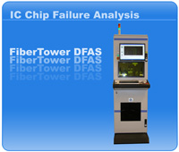
As an advancement to traditional ink marking, the nd:YAG laser was the earliest laser to be used for wafer marking. The nd:YAG laser is still the most common in the industry; however, manufacturers are now, more than ever, focused on improving processes to reduce costs and increase throughput, thereby increasing profitability. The lower cost of ownership (COO) and higher throughput of fiber laser marking systems compared to the YAG laser and traditional ink marking makes fiber laser systems very appealing.
Lower Costs, Higher Throughput
Manufacturing and material processing equipment can be very expensive; especially when your process contains two or more different applications. A unique benefit of fiber laser systems is that one laser can operate different processes with the use of an optical switch. For example, a manufacturer can operate cutting, marking and welding machines all off of the same fiber laser. This is especially beneficial to companies who are experiencing growth or looking to move into different processing markets.
Manufacturing and material processing equipment can be very expensive; especially when your process contains two or more different applications. A unique benefit of fiber laser systems is that one laser can operate different processes with the use of an optical switch. For example, a manufacturer can operate cutting, marking and welding machines all off of the same fiber laser. This is especially beneficial to companies who are experiencing growth or looking to move into different processing markets.
As production increases or new applications need to be implemented a manufacturer can also upgrade their laser wattage easily and affordably. Since the laser itself is the most expensive component of a system, manufacturers can save a considerable amount of money while expanding their operation in a more exponential manner. Additionally, the average diode life for Co2 and nd:YAG lasers is approximately 10,000 to 20,000 hours. Fiber lasers have an astonishing 50,000 to 100,000 hour diode life. A longer diode life, means less maintenance and less down time to change out the diode allowing your production to continue.
Compared to Co2 and nd:YAG laser systems, fiber laser systems do not require the use of consumables in their operation and are approximately 20 times more energy efficient. Both of these factors not only help manufacturers become more eco-friendly but are also key to reducing operating costs.
Production speed and throughput is a major concern for most manufacturers. The combination of speed, performance and versatility of fiber laser systems cannot be matched by any other marking technique. Fiber lasers offer high throughput due to the fiber-to-fiber architecture presenting a robust, monolithic design with no optics to align or maintain, no mechanics to stabilize, and high power densities are able to process even the most demanding applications. This allows manufacturers to increase the rate they process materials while not having to compromise any quality.
Semiconductor Industry Applications
 Portable digital components, cell phones, PDAs, and digital cameras become smaller and more lightweight but continue to increase in functionality. The Direct Chip Attach (DCA) or flip chip produces a need for wafer identification and tracking. Laser marking a wafer before it has been diced and processed enables manufacturers to trace defective parts. Due to the ever shrinking size of chips, the ability of a fiber laser to produce a small spot size weighs in heavily. Utilizing laser marking, as opposed to ink marking, is the best solution because it provides a mark that is permanent, readable, and of a enough high quality to meet even the most stringent requirements.
 Portable digital components, cell phones, PDAs, and digital cameras become smaller and more lightweight but continue to increase in functionality. The Direct Chip Attach (DCA) or flip chip produces a need for wafer identification and tracking. Laser marking a wafer before it has been diced and processed enables manufacturers to trace defective parts. Due to the ever shrinking size of chips, the ability of a fiber laser to produce a small spot size weighs in heavily. Utilizing laser marking, as opposed to ink marking, is the best solution because it provides a mark that is permanent, readable, and of a enough high quality to meet even the most stringent requirements.
Flat Panel Display Industry Applications
 Traditional methods to mark glass panels with tracking codes such as mechanical etching can crack the surface of the glass thereby compromising the overall strength and quality of the glass. These cracks can potentially lead to panel issues in the future. Additionally, the marks are not always clear enough to be scanned or easily read. Although laser marking technology has been around since the 1970s, it has been slow to replace traditional methods. But, the combination of speed, permanence, and reliability, is making manufacturers stand up and take notice when high throughput, time savings and lower costs are clearly the focus for flat panel display manufacturers.
 Traditional methods to mark glass panels with tracking codes such as mechanical etching can crack the surface of the glass thereby compromising the overall strength and quality of the glass. These cracks can potentially lead to panel issues in the future. Additionally, the marks are not always clear enough to be scanned or easily read. Although laser marking technology has been around since the 1970s, it has been slow to replace traditional methods. But, the combination of speed, permanence, and reliability, is making manufacturers stand up and take notice when high throughput, time savings and lower costs are clearly the focus for flat panel display manufacturers.
Solar Industry Applications
 Typically, consumers require 20 to 25 year warranties on solar panels. Therefore, wafer marking in solar cell manufacturing for traceability is a must. Traditional methods to mark panels with tracking codes such as mechanical etching or engraving using a Co2 laser can crack or chip the surface of the glass thereby compromising the overall strength and quality of the glass. Due the harsh environments the panels must endure, these imperfections can potentially lead to panel issues in the future affecting panel longevity.
Overall, fiber laser marking has proven to be the best solution to chip and wafer manufacturers, because it produces a permanent, readable, and high quality mark fulfilling manufacturers marking's most stringent requirements. And finally, the lower cost of ownership (COO) and higher throughput of fiber laser marking systems can’t be ignored in these tough economic times.
Fonon DSS, the cutting edge developer of state-of-the-art, laser scribing, dicing, marking, coating removal, direct patterning, and photo mask repair solutions for the Flat Panel Display (FPD), Semiconductor, Photovoltaic and Electronics industries throughout the world. For more information about Fonon DSS’ systems, please visit http://www.fonondss.com/ or call 407-829-2613.
Media Contact:
Maureen McHale
mmchale@laserphotonics.com
407-829-2613 x317
Media Contact:
Maureen McHale
mmchale@laserphotonics.com
407-829-2613 x317